Conferences
Peer-reviewed papers in international conference proceedings. See all publications →
25 entries
2026
-
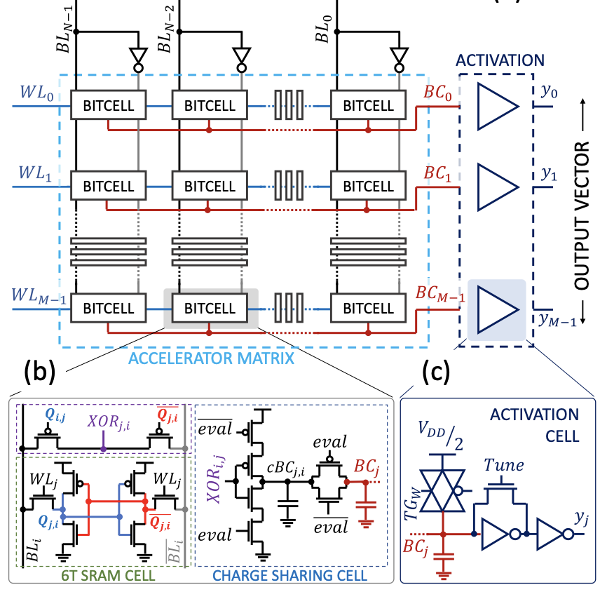 SRAM-Based Processing-in-Memory Cell Enabling Binary Neural Networks Through XNOR Multiplication and Charge-Domain Accumulation to be presented at IEEE International Conference on Electronics, Circuits and Systems (ICECS), 2026...
Loading… -
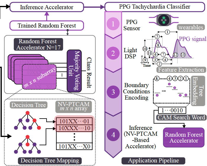 Reliability and Assessment of an MRAM-based Non-Volatile Precharge-Free Ternary CAM for Real-Time Edge Inference to be presented at IEEE Cross-Disciplinary Conference on Memory-Centric Computing (CCMCC), 2026Non-volatile content-addressable memories (NVCAMs) based on magnetic tunnel junctions (MTJs) are emerging as a compelling processing-using-memory (PuM) scheme for energy-efficient, massively-parallel pattern matching in AI inference and edge-computing workloads. This paper presents a comprehensive reliability and application-level study of a hybrid MTJ-CMOS NV precharge-free ternary CAM (NV-PTCAM) designed in a commercial 65 nm CMOS process. At the circuit level, we evaluate the impact of the number of ternary ‘don’tcare’ (X) states stored within the NV-TPCAM, and the impact of row segmentation. NV-PTCAM achieves a search delay below 0.25 ns, a search energy consumption of 1.82 fJ/cell, and a search error rate of about 0.02%, outperforming conventional NV-NOR and NV-NAND counterparts by up to 82% in search energy and up to 11.5× in search delay, on average. We apply an endurance model to the NV-PTCAM search workload and demonstrate that the number of cycles to failure exceeds 1013 for pulse amplitudes as high as 0.656V and pulse widths in the range 100- 500 ps, establishing the practical reliability of the NV-PTCAM for explainable artificial intelligence (xAI) models useful in wearable or edge devices. At the application level, we demonstrate the NV-PTCAM as the PuM inference engine of a real-time photoplethysmography (PPG)-based tachycardia classifier. The NV-PTCAM-based Random-Forest-based PuM system achieves a mean accuracy of 94.8% and an F1-score of 86.7% on the BIDMC clinical dataset, while the low SER of the NV-PTCAM has a negligible impact on classification performance.
Loading… -
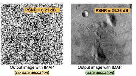 IMAP: In-MRAM Associative Processor with reliable bit-serial massively-parallel arithmetic operations Spintronics and Nanomagnetism Conference - SPIE Photonics Europe (INVITED), 2026The ever-growing demand for data-intensive applications has driven the adoption of in-memory computing (IMC) as a promising paradigm to overcome the von Neumann bottleneck of conventional computing architectures. Among the emerging memory technologies explored for IMC-based architectures, magnetic random-access memory (MRAM) stands out due to its non-volatility, high endurance, and compatibility with standard CMOS fabrication process. This work presents IMAP, an in-MRAM associative processor based on perpendicular anisotropy double-barrier magnetic tunnel junctions (DMTJs) with two reference layers. IMAP presents processing units built with NAND-type content-addressable memory (CAM) architecture, allowing bit-serial massivelyparallel arithmetic operations. Reliable and energy-efficient in-memory computing operations are achieved by properly carrying out a data allocation technique to mitigate variability-induced errors arising from the limited ratio between high-resistance and low-resistance states. IMAP is designed using a commercial 28 nm process and a Verilog-A-based compact DMTJ model calibrated with experimental physical parameters. Circuit-level Monte Carlo simulations demonstrate correct operation under worst-case conditions and show that the proposed data allocation increases the probability of correct 8-bit full-adder operations for the most significant bits from about 63% to approximately 95%. At the application level, IMAP is evaluated as an accumulator in a fixed-point twodimensional convolution workload, where the proposed approach improves the output peak signal-to-noise ratio from 6.21 dB to 24.26 dB. The obtained results indicate that IMAP can efficiently accelerate arithmetic kernels associated with contemporary data-centric applications, thereby suggesting MRAM-based associative processing as a potential IMC architecture for future memory-centric computing systems.
Loading… -
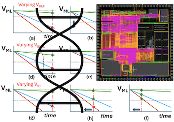 PatBiNN: A 65nm Processing-in-CAM Based BNN Implementation for Pathogen Genome Classification 2026 Design, Automation & Test in Europe Conference (DATE), 2026Binary Neural Networks (BNNs) are a cost-effective and highly efficient alternative to traditional neural networks. Genome classification is a frequent component of genome analysis pipelines, with a variety of applications spanning pandemic preparedness, AMR resistance control, drinking water and food safety. PatBiNN is a BNN based pathogen genome classifier optimized for edge and field use. It employs a binary multilayer perceptron (MLP) implemented using in-Hamming distance tol- erant (similarity search) content addressable memory processing. PatBiNN was designed and manufactured in a commercial 65nm process. It achieves F1 score of 88%, ROC AUC of 0.986, throughput of 0.8M inferences/s, power consumption of 4.8 mW and energy efficiency of 237TOPs/s/W with silicon area of 0.87mm2.
Loading…
2025
-
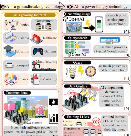 Hardware Accelerators For A Sustainable AI Future IEEE International Conference on Application of Information Technologies in Engineering, Management and Science (ICAI-TEMS), 2025The exponential growth of the use of artificial intelligence (AI) in all sectors of our society is driving unprecedented energy consumption and carbon dioxide emissions, threatening both the environment and the scalability of future AI technologies. This growing concern is especially pronounced in the context of transformer-based generative AI models, whose computational and energy demands continue to escalate rapidly. Addressing this challenge necessitates a shift from contemporary computing through the integration of novel computing paradigms and specialized hardware accelerators that significantly improve performance-per-watt efficiency. This work discusses the power-intensive nature of generative AI technologies, reviews current trends in AI hardware, and provides a forward-looking perspective on hardware accelerators, with a particular emphasis on memory-centric computing, specifically optimized for AI applications. By reviewing algorithmic and architectural advances, this work shows the central role of hardware innovation in enabling energy-efficient and scalable generative AI systems.
Loading… -
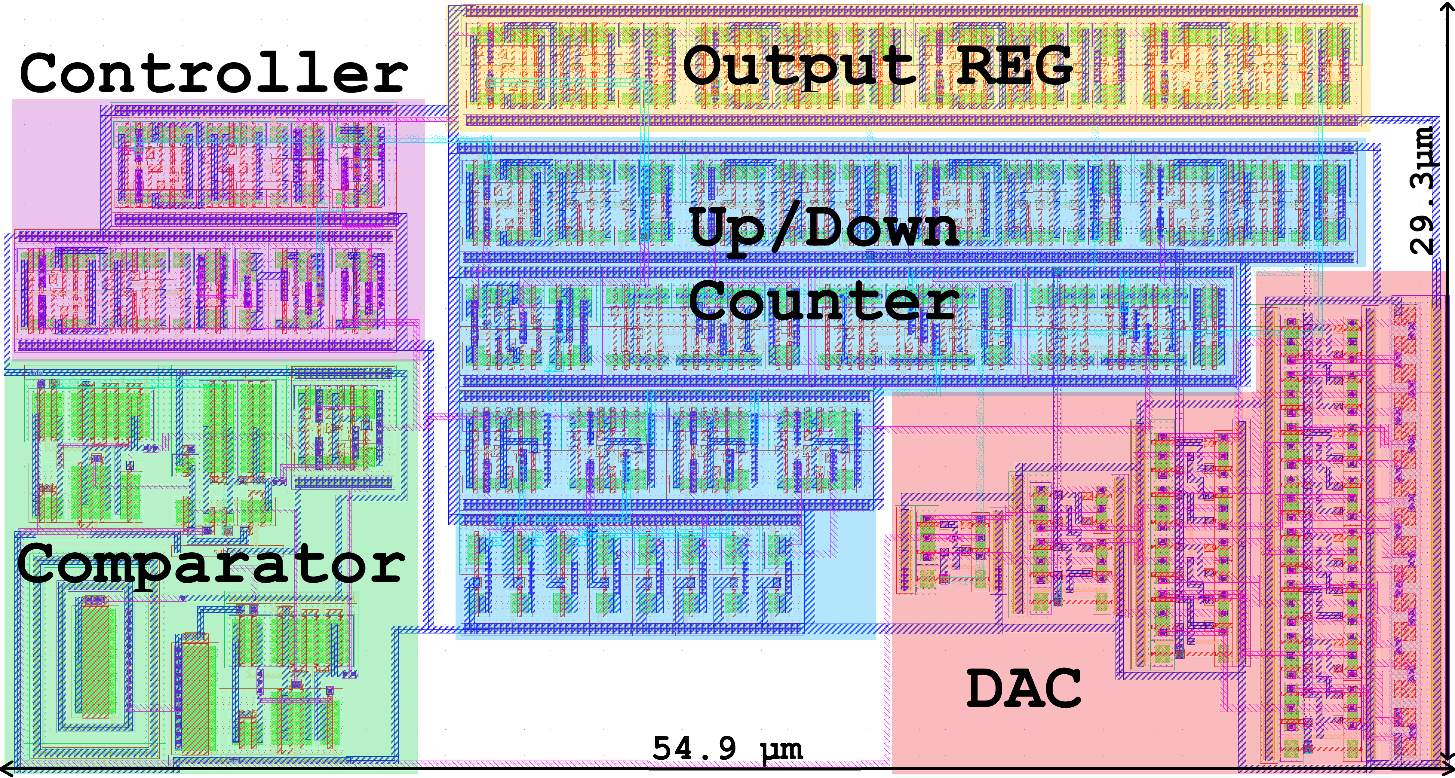 A Low-Power 4-bit Tracking-Type Analog-to-Digital Converter in SKY130 Process IFIP/IEEE International Conference on Very Large Scale Integration (VLSI-SoC), 2025This paper presents the design and full-custom layout implementation of a 4-bit Tracking-Type Analog-to-Digital Converter (TT-ADC) using the SKY130 130 nm CMOS process. The proposed architecture mainly integrates a rail-to-rail analog comparator and a multiplexed resistor-string Digital-to-Analog Converter (DAC), combined with a synchronous controller and an output register. Unlike traditional tracking ADCs, this work introduces a fully integrated mixed-signal design optimized for both bandwidth and power efficiency, and evaluated under process-temperature-voltage variations accounting for layout parasitics. Simulations show that the proposed TT-ADC presents a bandwidth of 150 MHz while consuming only 505μ W of power. Compared to prior 4-bit implementations, the proposed design achieves over 2× improvement in bandwidth and an 87% reduction in power consumption. The area footprint is about 54.9μm×29.3μm, making it highly suitable for energyconstrained, high-speed embedded applications.
Loading… -
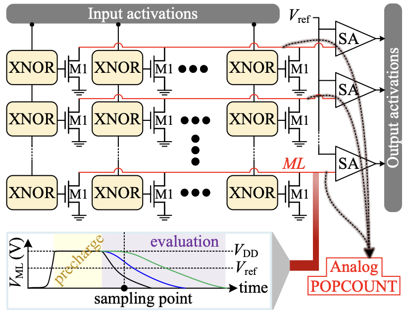 PiC-BNN: A 128-kbit 65nm Processing-in-CAM-Based End-to-End Binary Neural Network Accelerator IEEE Cross-Disciplinary Conference on Memory-Centric Computing (CCMCC), 2025Binary Neural Networks (BNNs), where weights and activations are constrained to binary values (+1, -1), are a highly efficient alternative to traditional neural networks. Unfortunately, typical BNNs, while binarizing linear layers (matrix-vector multiplication), still implement other network layers (batch normalization, softmax, output layer, and sometimes the input layer of a convolutional neural network) in full precision. This limits the area and energy benefits and requires architectural support for full precision operations. We propose PiC-BNN, a true end-to-end binary in-approximate search (Hamming distance tolerant) Content Addressable Memory based BNN accelerator. PiC-BNN is designed and manufactured in a commercial 65nm process. PiC-BNN uses Hamming distance tolerance to apply the law of large numbers to enable accurate classification without implementing full precision operations. PiC-BNN achieves baseline software accuracy (95.2%) on the MNIST dataset and 93.5% on the Hand Gesture (HG) dataset, a throughput of 560K inferences/s, and presents a power efficiency of 703M inferences/s/W when implementing a binary MLP model for MNIST/HG dataset classification.
Loading… -
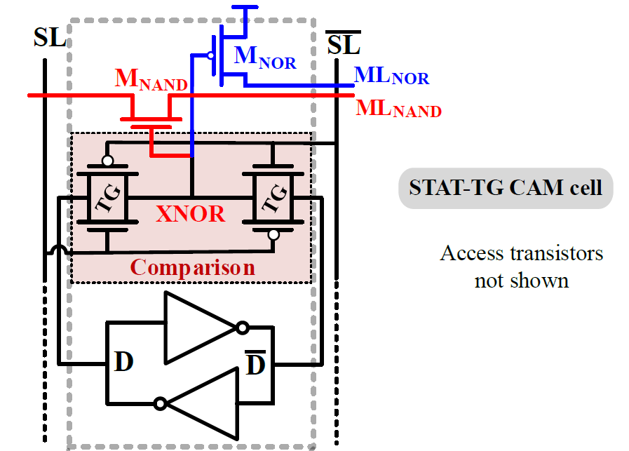 Towards Low-Power High-Performance Content-Addressable Memory: a Robust Precharge-Free Approach IEEE International Symposium on Circuits and Systems (ISCAS), 2025Low-power high-performance content-addressable memories (CAMs) are important components in modern computing systems. In this work, we present a robust CAM that overcomes the power and performance limitations of conventional precharge-based CAMs. The proposed static transmission gatebased (STAT-TG) CAM design achieves low-power operation comparable to NAND CAMs while maintaining search speeds rivaling those of NOR CAMs. The STAT-TG CAM was designed using a 65nm CMOS technology and comprehensively evaluated under extensive Monte Carlo simulations. Compared to conventional CAMs, the STAT-TG CAM is 14% faster than NAND CAM, while consuming only 25% of the energy per operation relative to NOR CAM. This makes STAT-TG CAM a promising solution for high-performance yet energy-efficient applications.
Loading… -
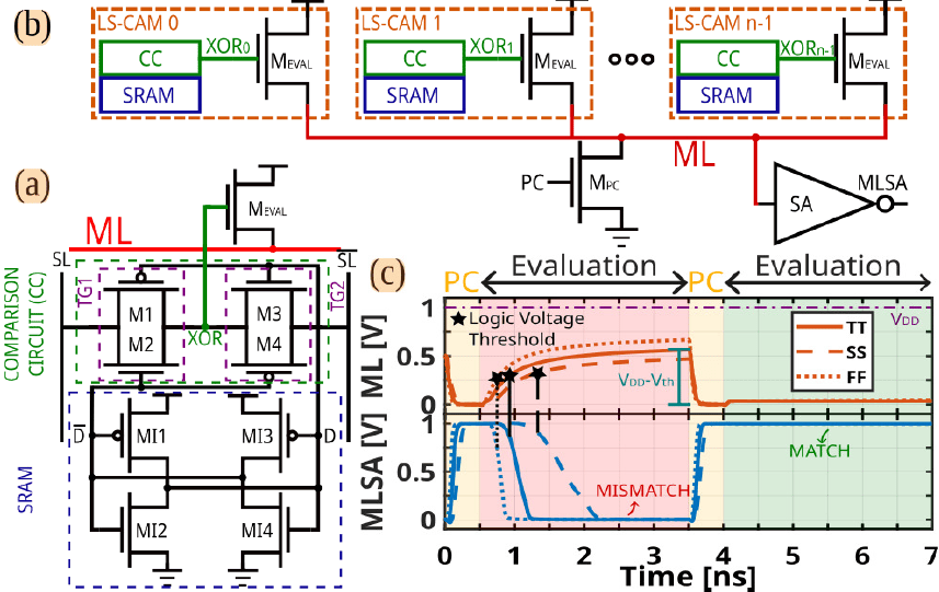 Low Matchline Voltage Swing Content-Addressable Memory Cell IEEE International Symposium on Circuits and Systems (ISCAS), 2025Content-addressable memory (CAM) is a specialized memory architecture designed for fast data searches, allowing a one-clock-cycle comparison between the search input and the entire memory content. In this work, a low matchline voltage swing CAM is proposed to reduce the search power consumption while maintaining high-speed search operations. Low voltage swing in the matchline is enabled by introducing extra circuitry in the conventional CAM cell. By means of comprehensive Monte Carlo and post-layout simulations using a commercial 65 nm node, we show that the proposed CAM cell design allows for robustness against process, voltage, and temperature variations without the need for dedicated matchline sense schemes. Compared to conventional precharge high NOR-type CAM, the proposed design achieves 42% higher speed and 29.1% less energy consumption. Post-layout results demonstrate that the proposed CAM operates reliably at 0.6V, maintaining performant and reliable search operations across a wide temperature range.
Loading… -
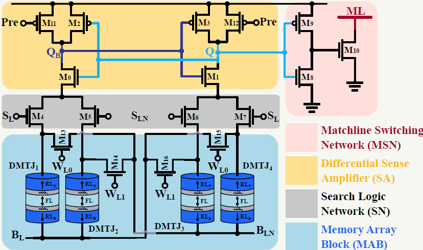 Non-Volatile Content-Addressable Memory for Energy-Efficient & High-Performance Search and Update Operations IEEE International Symposium on Circuits and Systems (ISCAS), 2025This work presents a non-volatile contentaddressable memory (NV-CAM) based on double-barrier magnetic tunnel junction technology (DMTJ). Unlike state-ofthe- art NV-CAM designs that present low-performance updates, our NV-CAM allows energy-efficient, high-performance search and update operations. This makes it well-suited for applications requiring a high frequency of searches/updates, such as associative processors. The NV-CAM hybrid CMOS/DMTJ was designed using a commercial 65nm CMOS technology and a Verilog-A-based DMTJ compact model. The NV-CAM evaluation was carried out by employing Monte Carlo simulations while accounting for process variations. Simulation results show that our NV-CAM presents competitive figures of merit compared to state-of-the-art design. Our NV-CAM presents energy-efficient operations and reduces the update and search delay by about 71% and 75%, respectively, compared to other NV-CAMs.
Loading…
2023
-
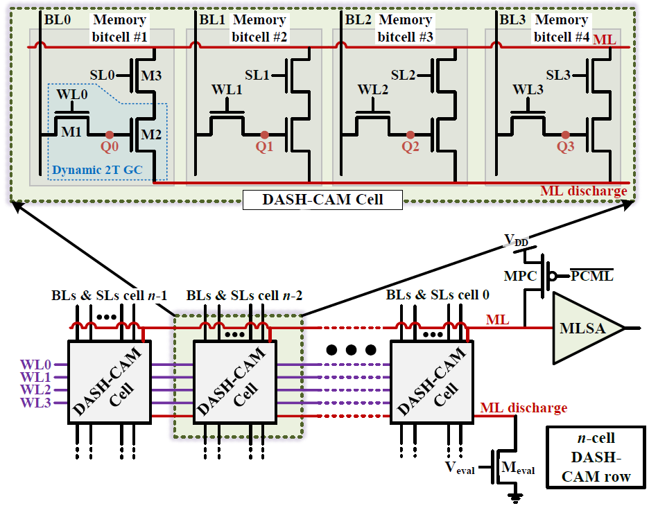 DASH-CAM: Dynamic Approximate SearcH Content Addressable Memory for genome classification Proceedings of the 56th Annual IEEE/ACM International Symposium on Microarchitecture (MICRO), 2023We propose a novel dynamic storage-based approximate search content addressable memory (DASH-CAM) for computational genomics applications, particularly for identification and classification of viral pathogens of epidemic significance. DASH-CAM provides 5.5 × better density compared to state-of-the-art SRAM-based approximate search CAM. This allows using DASH-CAM as a portable classifier that can be applied to pathogen surveillance in low-quality field settings during pandemics, as well as to pathogen diagnostics at points of care. DASH-CAM approximate search capabilities allow a high level of flexibility when dealing with a variety of industrial sequencers with different error profiles. DASH-CAM achieves up to 30% and 20% higher F1 score when classifying DNA reads with 10% error rate, compared to state-of-the-art DNA classification tools MetaCache-GPU and Kraken2 respectively. Simulated at 1GHz, DASH-CAM provides 1,178× and 1,040× average speedup over MetaCache-GPU and Kraken2 respectively.
Loading… -
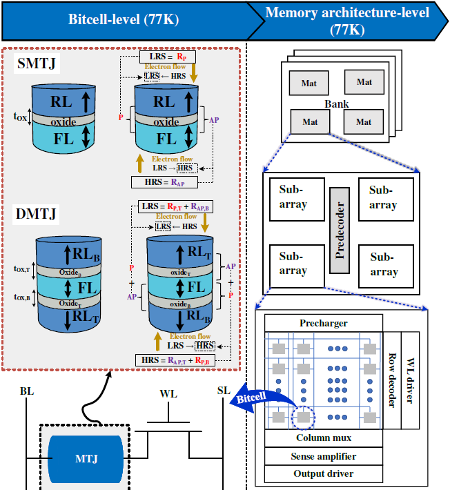 STT-MRAM Technology For Energy-Efficient Cryogenic Memory Applications IEEE 14th Latin America Symposium on Circuits and Systems (LASCAS), 2023This work explores non-volatile (NV) embedded memories implemented by spin-transfer torque magnetic random access memories (STT-MRAMs). Our designs are based on state-of-the-art perpendicular magnetic tunnel junctions (MTJs) along with a commercial 65 nm planar CMOS Bulk technology node, both operating at the liquid nitrogen temperature, 77 K. We evaluate the impact of cooling down to 77 K of the STT-MRAMs based on single- and double-barrier MTJ (SMTJ and DMTJ), and DMTJ with the relaxed non-volatility. All NV designs were benchmarked against the six-transistor SRAM (6T-SRAM) baseline. Simulation analysis relies on a 512 kB cache memory operating at 77 K. Overall, results show that the implementation of STT-MRAMs with DMTJ devices, and in particular when using the non-volatility approach by reducing the cross-section area, excel in terms of energy consumption, leading to energy savings for write/read access of about 35%/54%. This saving is obtained while also dissipating less leakage power and requiring a smaller bitcell footprint. Moreover, it presents reduced write latency overhead (as much as 1.9× lower), at the expense of increased read latency and reduced sensing margins of about 1.8× and 88%, respectively. The results suggest that STT-MRAM technology can be a solid alternative for energy-efficient cryogenic memory applications.
Loading… -
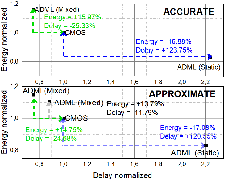 Exploiting Dual Mode Logic for Approximate Computing IEEE Seventh Ecuador Technical Chapters Meeting (ETCM), 2023The unique ability of dual-mode logic (DML) to self-adapt to computational needs by providing high speed and/or low-energy consumption is demonstrated for the first time for exact or approximate operations suitable for both error-resilient and exact applications. At the gate level, the DML design offers the possibility to operate either in the static mode to save energy or in the dynamic mode to increase speed, albeit with higher delay or energy consumption, respectively. In this paper, these two operation modes of the DML gates are optimally managed by a self-adjustment mechanism to increase speed or reduce the energy at run time, while changing the design accuracy. As a test case, a DML Carry Look Ahead adder (CLA) based in Dual Mode Logic (DML) that can operate in exact and approximate mode with the same frequency has been proposed. Through comparisons with CMOS-based alternative at various operating voltages, the advantages of the ADMLCLA are showcased. In static mode, the ADML-CLA presents less energy consumption of about 16% to 21%. In mixed mode, the ADML-CLA achieves delay reduction of 21% to 25%. The effectiveness of the controller in saving energy is demonstrated, with the ADML-CLA consuming less energy than CMOS when static signals are prevalent. Monte Carlo simulations highlight the lower average delay and deviation of the ADML-CLA compared to CMOS. Evaluation at a nominal voltage of 0.4V shows that the ADML (mixed) outperforms CMOS in terms of energy-delay product (EDP) in both exact and approximate modes.
Loading…
2022
-
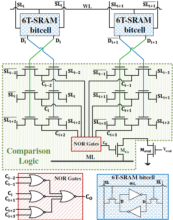 EDAM: Edit distance tolerant approximate matching content addressable memory Proceedings of the 49th Annual International Symposium on Computer Architecture (ISCA), 2022We propose a novel edit distance-tolerant content addressable memory (EDAM) for energy-efficient approximate search applications. Unlike state-of-the-art approximate search solutions that tolerate certain Hamming distance between the query pattern and the stored data, EDAM tolerates edit distance, which makes it especially efficient in applications such as text processing and genome analysis. EDAM was designed using a commercial 65 nm 1.2 V CMOS technology and evaluated through extensive Monte Carlo simulations, while considering different process corners. Simulation results show that EDAM can achieve robust approximate search operation with a wide range of edit distance threshold levels. EDAM is functionally evaluated as a pathogen DNA detection and classification accelerator. EDAM achieves up to 1.7x higher F1 score for high-quality DNA reads and up to 19.55x higher F1 score for DNA reads with 15% error rate, compared to state-of-the-art DNA classification tool Kraken2. Simulated at 667 MHz, EDAM provides 1, 214× average speedup over Kraken2. This makes EDAM suitable for hardware acceleration of genomic surveillance of outbreaks, such as the ongoing Covid-19 pandemic.
Loading… -
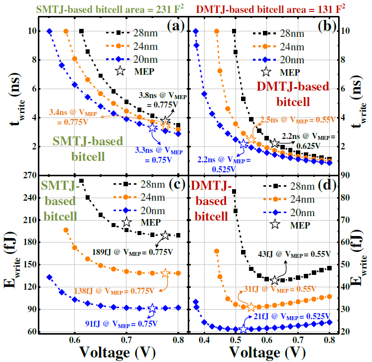 Voltage and technology scaling of DMTJ-based STT-MRAMs for energy-efficient embedded memories IEEE 13th Latin America Symposium on Circuits and System (LASCAS), 2022This work presents energy advantages allowed by the technology and voltage scaling of spin-transfer torque mag-netic random access memories (STT-MRAMs) based on perpen-dicular double-barrier magnetic tunnel junction (DMTJ), with two reference layers. DMTJ is benchmarked against the single-barrier MTJ (SMTJ) -based alternative, and a comprehensive evaluation is carried out through a cross-layer simulation frame-work, considering state-of-the-art Verilog-A based SMTJ and DMTJ compact models, along with a 0.8V FinFET technology. Simulation results show that, thanks to the lower voltage op-erating point, DMTJ-based STT-MRAM allows energy savings for write/read operations of about 38%/45%, as compared to its SMTJ-based counterpart. Moreover, scaling from the 28 nm down to the 20 nm node, the DMTJ-based memory cell improves write/read energy of about 29%/33% at the expense of longer access times.
Loading… -
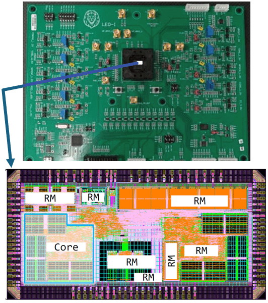 A RISC-V-based research platform for rapid design cycle IEEE International Symposium on Circuits and Systems (ISCAS), 2022This work proposes a novel platform for bringing a project from the concept to the tapeout stage in a short amount of time. An open-source and extendable RISC-V architecture is exploited to build a small area footprint core. This leads the research platform to be flexible in terms of design integration, while also allowing fast design cycles of research chips.
Loading…
2020
-
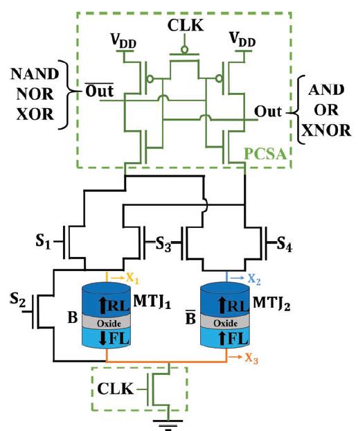 Reconfigurable CMOS/STT-MTJ Non-Volatile Circuit for Logic-in-Memory Applications IEEE 11th Latin American Symposium on Circuits & Systems (LASCAS), 2020The unique properties of spin-transfer torque magnetic tunnel junctions (STT-MTJs) have led to promising designs for logic and memory applications. Additionally, STT-MTJ based circuits have shown attractive potential to design efficient non-volatile logic-in-memory (NV-LIM) architectures, which assure low power and increased speed. This paper proposes a bit-level reconfigurable NV logic circuit based on hybrid CMOS/STT-MTJ design. Indeed, our circuit can adapt on-demand its structure, thus offering intrinsic flexibility to perform basic logic functions (i.e. AND/OR/XOR) by a single circuit architecture. Post-layout simulation results prove that the proposed circuit leads to increase both delay and energy consumption with respect to state-of-the-art non-reconfigurable designs. However, its reconfigurable operation capability is very attractive to reduce area occupation and to increase design flexibility of NV-LIM systems.
Loading…
2019
-
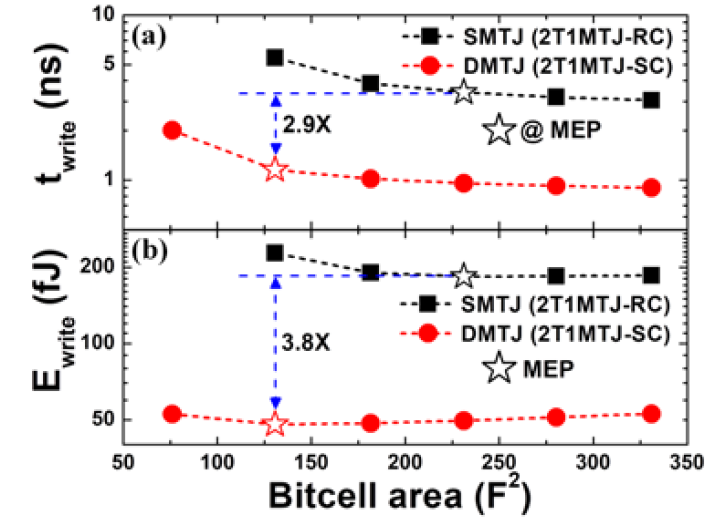
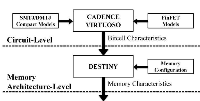 Exploiting Double-Barrier MTJs for Energy-Efficient Nanoscaled STT-MRAMs 16th International Conference on Synthesis, Modeling, Analysis and Simulation Methods and Applications to Circuit Design (SMACD), 2019This paper explores performance and technology-scalability of STT-MRAMs exploiting double-barrier MTJs (DMTJs) as comparatively evaluated with respect to conventional solution based on single-barrier MTJs (SMTJs). The comparative study was carried out at different design abstraction levels: (i) a bitcell-Ievel analysis relying on the use of Verilog-A compact models, and (ii) an architecture-level analysis for various memory sizes. Overall, our simulation results point out that, thanks to the reduced switching currents, DMTJ-based STT-MRAMs allow reducing write latency of about 60% than their SMTJ-based counterparts. This is achieved while assuring lower energy consumption under both write (-40%) and read (-27%) accesses, at the cost of reduced sensing margins.
Loading… -
 Evaluating the Energy Efficiency of STT-MRAMs Based on Perpendicular MTJs with Double Reference Layers 13th IEEE International Conference on ASIC (ASICON), 2019This paper evaluates the energy efficiency of STT-MRAMs based on double-barrier MTJs (DMTJs) as compared to conventional single-barrier MTJ (SMTJ) - based solutions. Our comparative study exploits a cross-layer simulation framework, which spreads from device-up to the architecture-level for different cache sizes. Owing to the reduced switching current, DMTJ-based STT-MRAMs prove to be credible candidates for next-generation non-volatile cache memories.
Loading… -
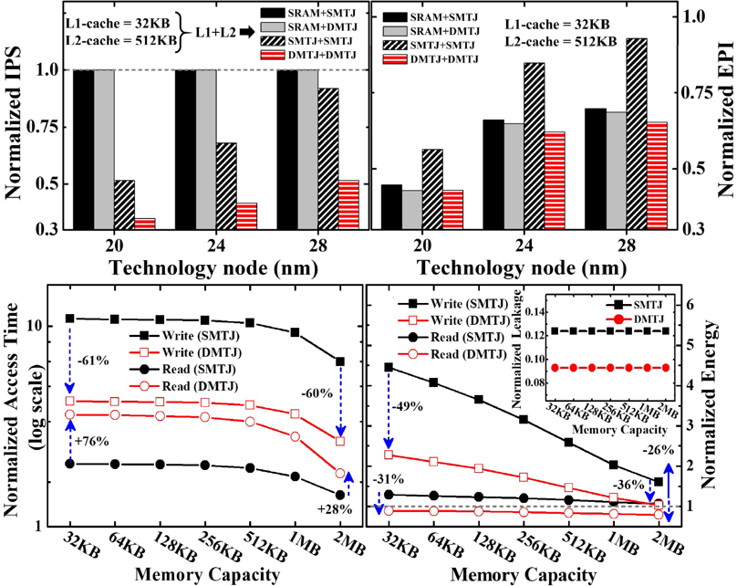 Device-to-System Level Simulation Framework for STT-DMTJ Based Cache Memory 26th IEEE International Conference on Electronics, Circuits and Systems (ICECS), 2019This paper presents a comparative study on non-volatile cache memories based on nanoscaled spin-transfer torque (STT)-magnetic tunnel junctions (MTJs). In particular, the impact of using double-barrier MTJs (DMTJs) instead of conventional single-barrier MTJs (SMTJs) is evaluated through a device-to-system level simulation framework. Simulation results demonstrate that DMTJ-based STT-MRAMs are promising competitors for the next generation of non-volatile cache memories.
Loading… -
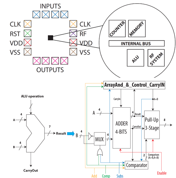 Microprocessor Design with a Direct Bluetooth Connection in 45nm Technology Using Microwind 10th IEEE Latin American Symposium on Circuits & Systems (LASCAS), 2019This paper presents the full-custom design of a 45nm microprocessor using the electronic design automation (EDA) software, Microwind. The design consists of fundamental modules: the arithmetic logic unit (ALU), memory, counter and an integrated Bluetooth (BT) port working at the 2.4 GHz. This design is validated by simulation under a process, voltage, and temperature (PVT) testing. The microprocessor can handle up to 4 bit since its purpose is focused on specific applications such as the internet of things (IoT). In order to communicate to the external world and with other devices, a strong input/output data interface and radio frequency (RF) transmission modules are implemented. Moreover, the RF module also contains a Bluetooth communication, which allows the wireless data transmission from/to the microprocessor.
Loading…
2018
-
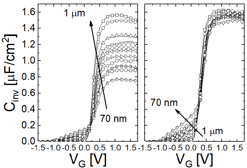 Capacitance Extraction of 34-nm Metallurgical Channel Length MOSFET for Parasitic Assessment Using the RFCV Technique 3rd IEEE Ecuador Technical Chapters Meeting (ETCM), 2018This paper presents the description and the results obtained with a new RFCV system written on python v2.7. which is used to acquire different parameters from MOSFET devices. RFCV is a technique that permits the measurement of capacitances from devices with an oxide thickness up into the nanometric range. Employing this technique, the developed system controls two tools in a synchronized way: a Vector Network Analyzer (VNA) and a Source Measure Unit (SMU) located in a Parameter Analyzer (PA). The obtained results are satisfactory and allow getting an adequate parameter extraction and the corresponding parasitic assessment of devices with channels as short as 34 nm.
Loading…
2016
-
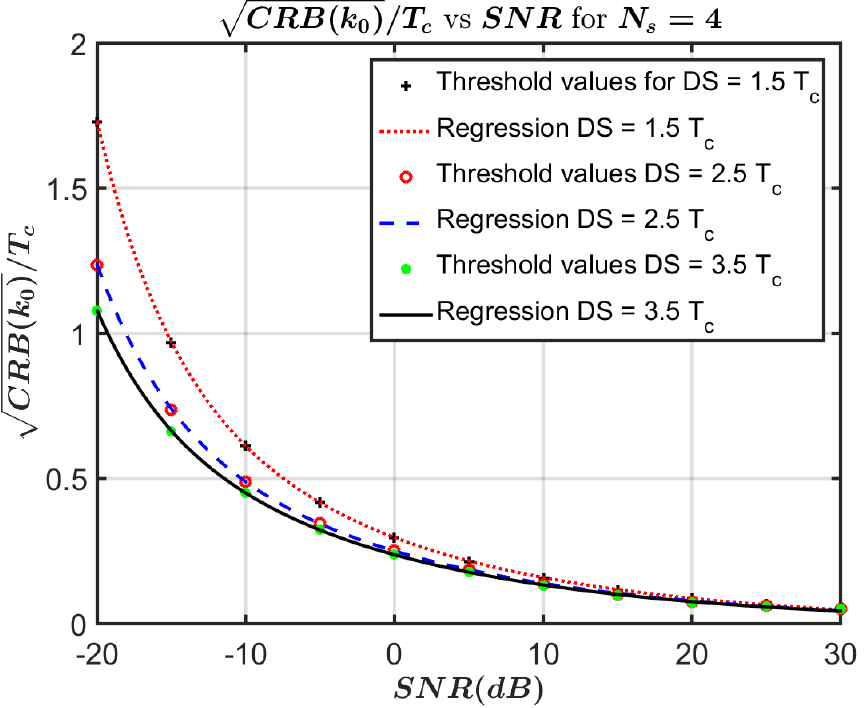 Fast computation of Cramer-Rao Bounds for TOA IEEE Latin American Conference on Computational Intelligence (LA-CCI), 2016As part of a larger scope work that studies network-based positioning, that employs timing measures, this article proposes a methodology to add Cramer-Rao Bounds (CRBs) information to the propagation model. Moreover, it enables a very quick computation of CRBs for timing, avoiding the growing computational effort resulting from Fisher's matrix formulation and its inversion for each required position at the simulation stage, assuring at the same time the reliability of the required data in the study of positioning using space-time diversity. This methodology considers the variability of the propagation conditions in terms of delay spread (DS) and Signal-to-Noise ratio (SNR) in a realistic scenario. It also coordinates the operation of concurrent models within simulation, and finally performs bi-exponential regression and interpolation procedures on pertinent operational regions for CRBs. Properly validated models provide simple closed expressions that ease the operational region discrimination and its integration to the positioning simulation platform.
Loading… -
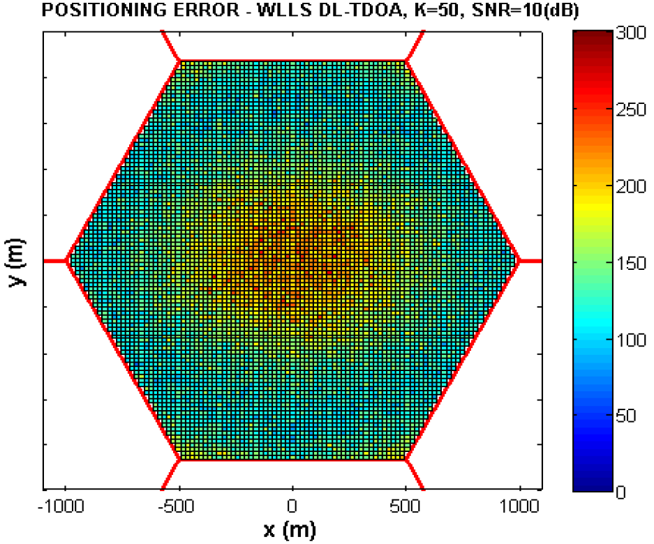 Space-time diversity for NLOS mitigation in TDOA-based positioning systems IEEE International Engineering Summit (IE-Summit), 2016This paper studies the potential impact of using space-time information in the mitigation of the Non-Line-Of-Sight condition in mobile subscriber's positioning systems. First of all, this work discusses the positioning problem based on measures of Time Differences Of Arrival departing from a more exact characterization of the signal statistics and including some geometrical restrictions to achieve an improved accurate. Furthermore, a novel approach that integrates signal propagation characteristics to information provided by a suitable timing estimation model based on Cramer Rao Bound for a Rayleigh-fading channel, when antenna arrays are used at the receiver and when a set of channel vector estimates are available, has been introduced to study the positive benefits of space-time diversity. These approaches are evaluated within a realistic simulation scenario.
Loading… -
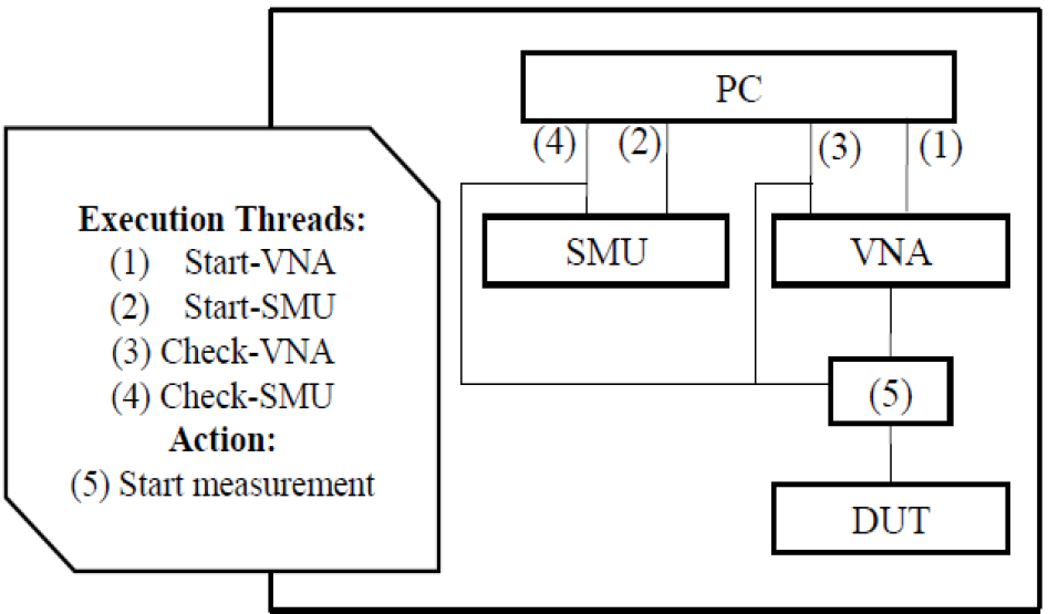 Remote control of VNA and parameter analyzer for RFCV measurements using Python IEEE Technical and Scientific Conference of the Andean Council (ANDESCON), 2016This paper presents the development of capacitance measurement with RF signal (RFCV) for MOSFET. Such technic is fundamental to measure and extract capacitances from nanometric range oxide thickness, which are very leaky in low frequency range measurements. This method uses the control and synchronization of a vector network analyzer (VNA) with a Source Measure Unit (SMU) from a parameter analyzer (PA). The control is established by a remote graphical interface developed in Python. It includes the use of standards like IEEE 488.2, SCPI and Ethernet link protocol. For the RFCV measurements, the SMU provides the DC voltage whereas the VNA the RF signal.
Loading…